The diffraction limit imposed by Heisenberg uncertainty principle can be overcome by a number of different approaches. In fact up to now quite a few superresolution optical microscope techniques have been developed. However, most of them use fluorophore dyes, require a comprehensive image integration, or result in large devices with the need for qualified users and costly maintenance [1-3].
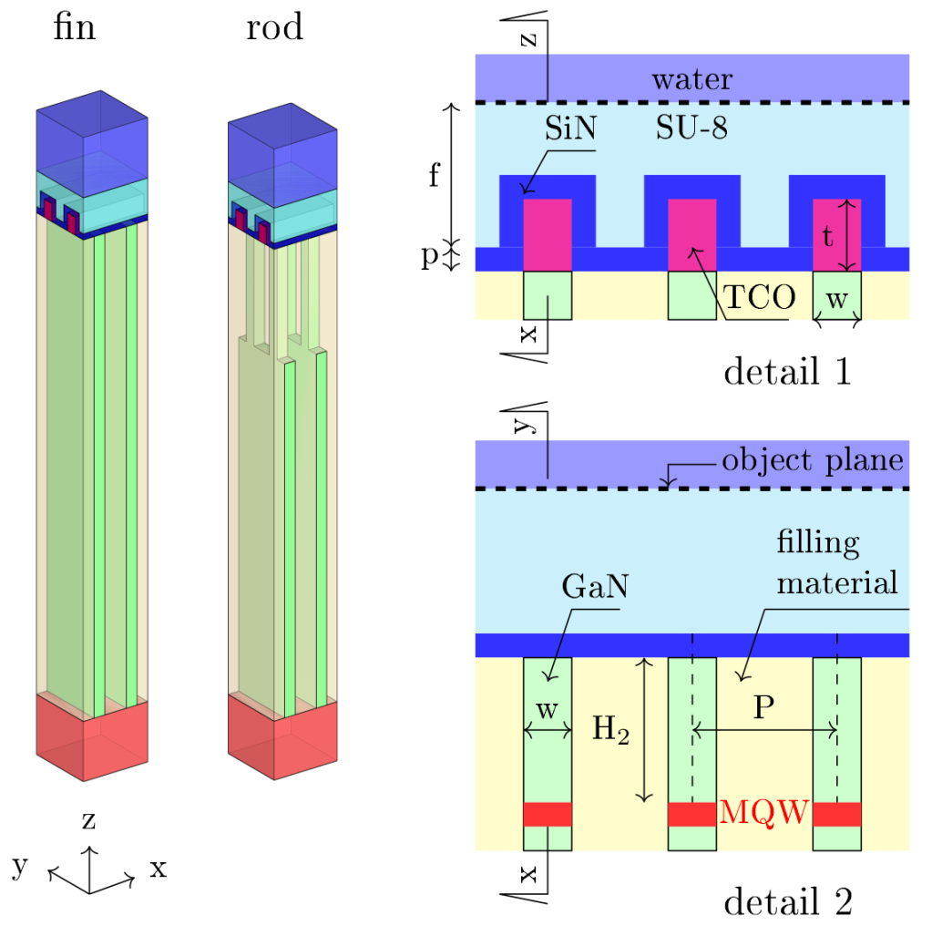
Looking toward the simplest possible lensless solution for superresolved imaging, we decided to analyse the capabilities of blue InGaN/GaN LED arrays as a highly resolved illumination engine. Each single LED can be switched on and off independently, locally illuminating the sample, which is assumed to be in the optical near field. The shadow image of the object is then collected by the detectors (e.g. CMOS Single Photon Avalanche Photodiode SPAD) [4]. Such arrays allowing for single pixel control are already being fabricated, but the LED size is still in the micrometer range. Here we present full wave optical simulations of nano sized LED arrays. In particular, we analyse two possible designs of LEDs, i.e. fins and rods, as can be seen on Fig.1.
Figure 1. Scheme of two designs of InGaN/GaN nanoLED array: fins and rods. Rods array is fabricated by etching the fins.
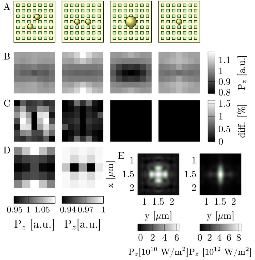
We are simulating the images (see Fig.2) of various gold nanoparticle arrangements collected by the proposed nano illumination microscope. The images are then analysed in order to understand the capabilities and limitations of the microscope and also to define the guidelines to obtain a highly resolved illumination engine.
Figure 2. (A) The schemes of the investigated Au nanoparticle arrangements. From the left: two nanoparticles of radius 50 nm separated by the distance of one array pitch, i.e. 100 nm and rotated by 60° along x axis, two nanoparticles of radius 50 nm separated by 100 nm laying along x axis, one nanoparticle of radius 50 nm located above the central LED and one nanoparticle of radius 100 nm once again placed above the central pixel. (B) Far field light intensity collected by the detector, while illuminating the above Au nanoparticles arrangements with each of the LEDs of the array one by one. (C) The related light pattern deviations from the symmetry across y=-x axis. (D) The light intensity patterns for dense (W=50 nm, P=100 nm, 1st) and sparse (W=100 nm, P=300 nm, 2nd) array in the case of two Au nanoparticles laying along x axis in one period distance. (E) Signal xy cross section in the image plane for the dense array and the sparse array, respectively.
A detailed description of the optical simulations and optimization of nanoLED array geometry will be presented at NUSOD-20. This work is a part of an European Horizon 2020 project Chipscope. More information about the project, in particular on the fabrication process of nanoLEDs, integration of nanoLED array into a chip and microfluidic chamber design can be found at the project website www.chipscope.eu.
[1] L. Novotny and B. Hecht, “Principles of Nano-Optics,” 2nd ed., Cambridge University Press, 2012.
[2] S. So, M. Kim, D. Lee, D. M. Nguyen, and J. Rho, “Overcomingdiffraction limit: From microscopy to nanoscopy,” Appl. Spectrosc. Rev.,vol. 53, pp. 290–312 (2018).
[3] E. Sezgin, “Super-resolution optical microscopy for studying membranes tructure and dynamics,” J. Phys. Condens. Matter, vol. 29, pp. 273001,2017
[4] J. Gülink, S. Bornemann, H. Spende, M. Auf der Maur, A. Di Carlo,J. D. Prades, H. S. Wasisto, and A. Waag, “InGaN/GaN nanoLED Arraysas a Novel Illumination Source for Biomedical Imaging and SensingApplications,” Proceedings, vol. 2, pp. 892, 2018.